Usually introductions to electronics include Ohm's Law, Kirchhoff's Current & Voltage Laws, and introductions to resistors, capacitors, and inductors. These are typically taught regarding ideal cases, in order to convey the basics, but this can fall short of the needs of real-world applications. The text I'm covering here, Applied Embedded Electronics by Jerry Twomey, works on an understanding that the reader understands most of the theoretical basics of electronics, and seeks to move quickly to the more practical aspects of embedded and high-frequency applications. The first section will skim the basics and draw attention to the less-than-ideal, though fully pragmatic aspects of components in real applications.
When do designers need to pay attention to the limitations of non-ideal devices? To decide this we need to build an awareness of common problems in applied electronics. To solve any problem, we must first accept that nothing is ideal.
Many texts want to cover the basics. This is not the central goal here. Rather, the goal of this text is to focus on what is necessary to design a reliable electronic system. If you are familiar with the following concepts, you should have the background to work with the following material.
Definitions for Resistance & Conductance
Ohm's Law and Ohm's Law for Alternating Current
Steady State DC System: A Steady State is when the operating condition of a circuit is constant. This doesn't mean that all current and voltage values are constant, but that their change is consistent, cyclical, and predictable. For example, a battery powered radio receiver can be said to be in a steady state while receiving from a station, since there is no drastic change after it is powered on, and circuit performance is predictable while processing a broadcast.
Steady State AC System: When a circuit is driven by sinusoidal power sources at a single frequency, the steady state voltages and currents are also sinusoidal, though at different phases and amplitudes from the power. Analysis in this kind of system is done with Phasors, which reduce to algebraic relationships rather than differential equations in time. This analysis is often used when planning power systems.
Transient Signals or Transient Response: This is the response or recovery of an electrical system from any disruption of its steady state. A transient disruption can originate internally or exogenously.
Decibels: The decibel is typcally used to describe power ratios, e.g. signal to noise in radio transmission. It also uses a logarithmic scale, where a positive change of 10dB represents a 10x increase in power. Some shorthand approximations include 3dB as a 2x change, and 6dB as a 4x change.
Time Domain vs. Frequency Domain: The most immediate example here is in how spectrograms display the frequency content of their reading. If a spectrogram is displaying in the frequency domain, you will see a graph of amplitudes for only the frequencies present in the spectrum at a given time. However, if it displays data in the time domain, we can observe a detailed history of changes in frequency amplitudes over time.
Fourier Series: The very base of the Fourier series and associated theorems is that a function, like a waveform, can be respresented as a sum of sinewaves or harmonics. An applicable example is a square wave. By taking the partial sum of relevant harmonics, the sum function gradually approaches a square wave. This concept is also used to perform the Fast Fourier Transform and take signals from their transmission domain (time or space) and display them in the frequency domain.
Harmonics: On a spectrogram, harmonics appear as positive integer multiples above the fundamental frequency, if that fundamental function is not a pure sinewave. These would appear as fainter lines or spikes on a graph, but these higher harmonics also produce the 'richness' of a signal, which is more easily demonstrable in the acoustic medium. A pure sinewave at A440 played by a speaker has no harmonics, and would appear as a single spike on a spectrogram, but the same pitch played by a violin would produce many additional harmonics, as the soundbox of the instrument resonates and projects these higher frequencies, and the action of the bow against the string creates more of a saw-tooth function, thus making a rich timbre rather than a pure sinewave.
LC Circuits: Also called Resonant Circuits, Tank Circuits, or Tuned Circuits, these consist only of an inductor and capacitor, and are used either to pick out the resonant frequency of the circuit, or to emit signals at a particular frequency. When picking a specific frequency out of a complex signal, their funcion is as a Bandpass Filter. They can also be configured as broader Low Pass or High Pass filters, only passing signals above or below a specific threshold.
RC Time Constant: This is the time-constant of a Resistor-Capacitor Circuit, and is equal to the product of the circuits resistance and capacitance. It is the time in seconds required to charge the capacitor through the resistor from zero up to roughly 62.3% of the applied voltage, or to discharge the capacitor through the resistor down to about 36.8% of the initial charge voltage. When calculating, the units for Resistance and Capacitance remain in Ohms and Farads respectively.
Modern electronic systems are primarily digital, but most design problems arise from the analog aspects of the same systems. These problems include noise, signal integrity, power stability, electromagnetic interference (EMI), and connection impedance. These can quickly render a system non-functional.
Digital systems are more tolerant to the listed problems, but they can still be broken by their analog limitations. The version of electronics and accompanying theory regularly taught can be thought of as first order models. They simplify some aspects to aid in understanding, but real 'second-order' effects can still affect real device performance. A more detailed model would aid engineers and result in better and more robust design. The techniques listed here are intended to deal with second order effects and to remedy them.
Even short pieces of wire can have significant intrinsic impedance. For example a 10cm segment of 24 AWG copper wire can have about 100nH (nano-Henrys) of inductance, 10 mili-Ohms (0.01Ω) of resistance, and capacitive coupling to its surroundings. In this example, the impedance and capacitance act as a low-pass filter in the surrounding environment for interference above the 300-400MHz range. This will also be sensitive to motion as capacitance will change as a function of the wire's position relative to the ground. [Tangent 1] A thicker wire can reduce resistance, parallel connections can reduce inductance (see ethernet and phone-line bundling) but overall inductance is not easily eliminated.
The analogous 10cm connection on a printed circuit board (PCB) will show very similar characteristics. Inductance is about the same as the wire, but there is more capacitance because the connection is tightly spaced over a ground plane (in standard fabricated PCBs). In this configuration the connection will start to act as a low pass filter for signals around 80-90MHz due to the increased capacitance. This connection would catch broadcast signals in the right position, and the other characteristics would not change with the positioning of the circuit.
The broad takeaway here is that every connection has some impedance and coupling to an outside environment.
Tangent 1: WHY exactly do these connections behave as low pass filters on ambient signals? The small 'parasitic' traits of the wire block higher-frequency noise above a cutoff frequency related to the combined traits, while lower frequencies can pass through. This is because the properties of the wire form a kind of 'wall' for the higher-frequency waves which stops or impedes their propagation.
When connecting things together in the next example, the impedance of the source, connection, and load influence how much signal loss happens. Signal loss and distortion get progressively more severe with longer connections and higher frequencies. Designs working under 50MHz and in boards smaller than a 10cm*10cm profile can ignore these phnomena and generally survive. High bandwidth, long distances, and non-PCB connections make interconnections a significant part of the design problem.
High frequency signals with lengthy connections are also subject to signal loss and transmission line characteristics. Again in a 10cm connection, current transits the wire in about 0.7 nanoseconds. Depending on the connection length and signal frequency, a poorly terminated line can also affect signal integrity.
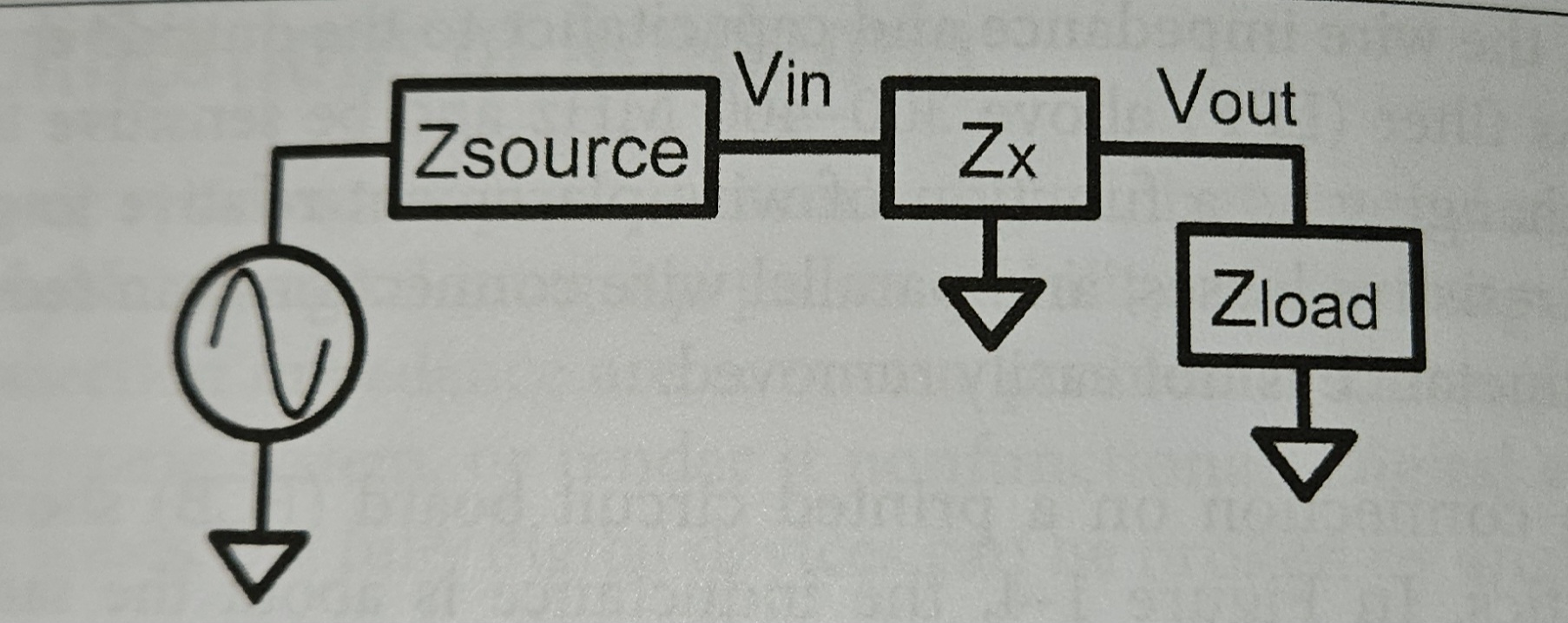
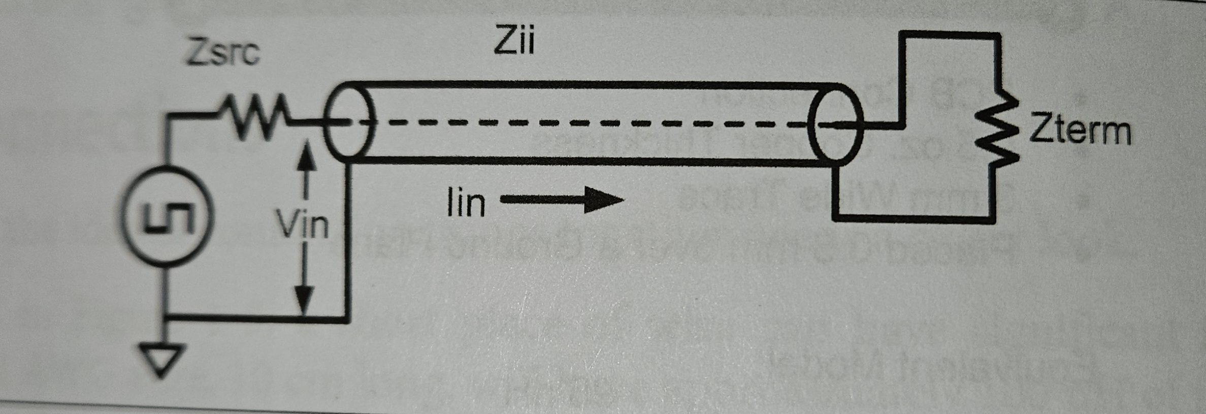
Designers must consider transmission line effects when the signal wavelength becomes a significant portion of the connection distance. For a 10cm wire, keeping wavelengths under 1/10th the length of the wire would limit signals to 280MHz sinusoid. A digital signal would have several harmonics above the fundamental to be included, which further limits the capability of the connection. Termination impedance (Zterm) should match characteristic input impedance (Zii) of the line to minimize reflection on the line. In practical use, both ends are terminated to minimize both initial and residual incidences of reflection. Impedance matching, striplines, and high-integrity data-paths will be covered in later installments.
Tangent 2: Why do digital signals have harmonics? Any signal that is not a pure sinewave will have harmonics in a medium because that signal can be decomposed into multiple other frequencies. Even a pure sinewave can create harmonics in a medium, provided that related resonators are present.
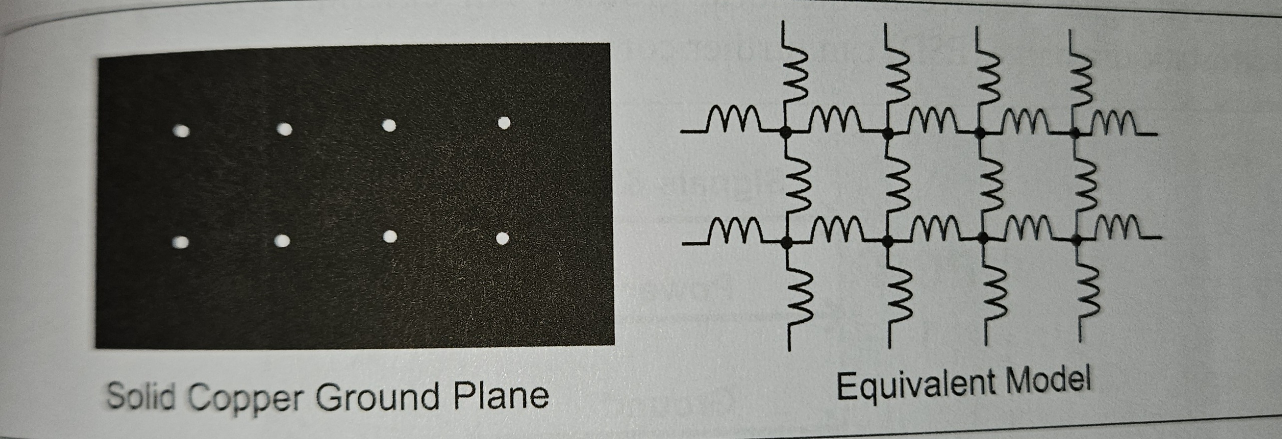
A solid copper ground plane in a PCB will exhibit some resistance and inductance between given points. Current at any point will cause a local voltage transition relative to the rest of the ground plane. A surge of current into a ground plane is like a person jumping on a trampoline. The ground 'bounce' can be kept low by minimizing ground impedance and ground-surge magnitudes. It should be noted that there is not a single ideal ground. The voltage of a 'ground' can vary, both with proximity of current passage points and the dynamics of the current passing through the ground medium.
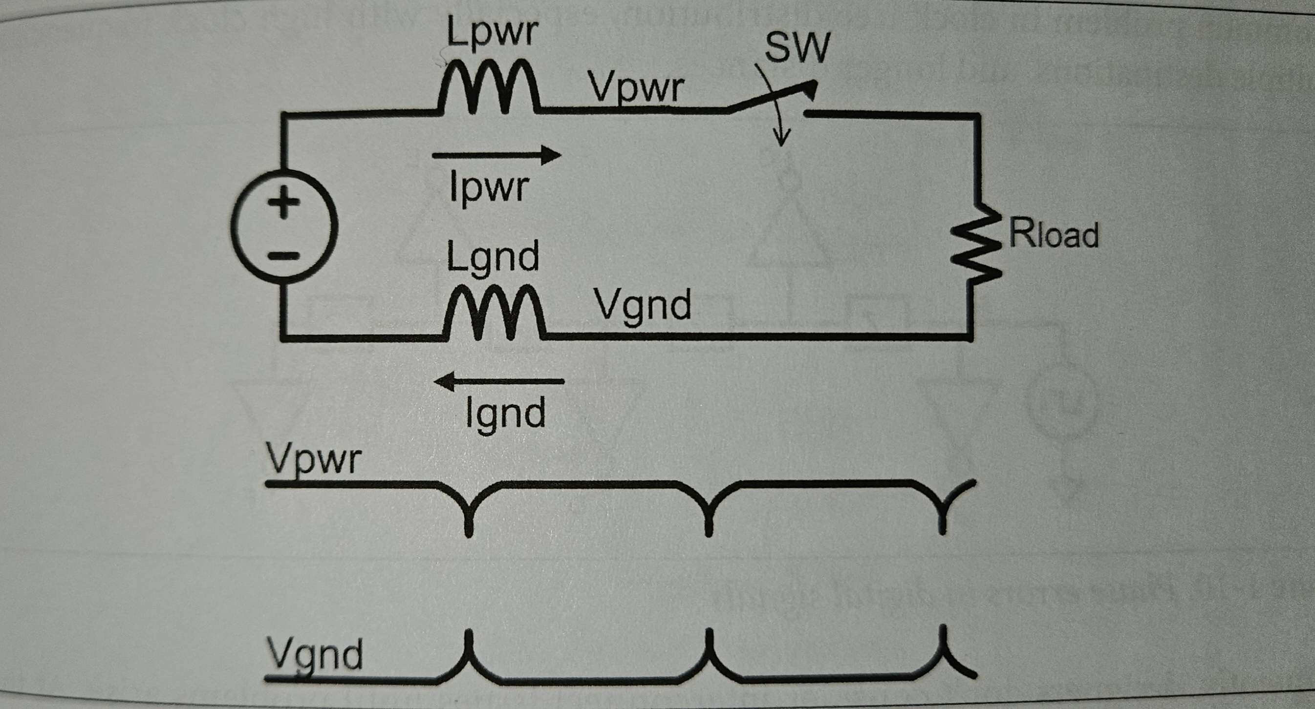
Power and ground connections have impedance. A switched load in an electronic device causes power voltage to drop, and ground voltage to rise. The magnitude of this variance is affected by the connection impedance and the transient rate-of-change of current. Transient current can change with the resistance-variance of the load, as well as capaitance across the load. A proper design adjusts these variables to provide power/ground stability, enough to keep proper function. In most cases, a power-ground bounce can be made manageable with proper techniques, including power bypass filtering and PCB layout.
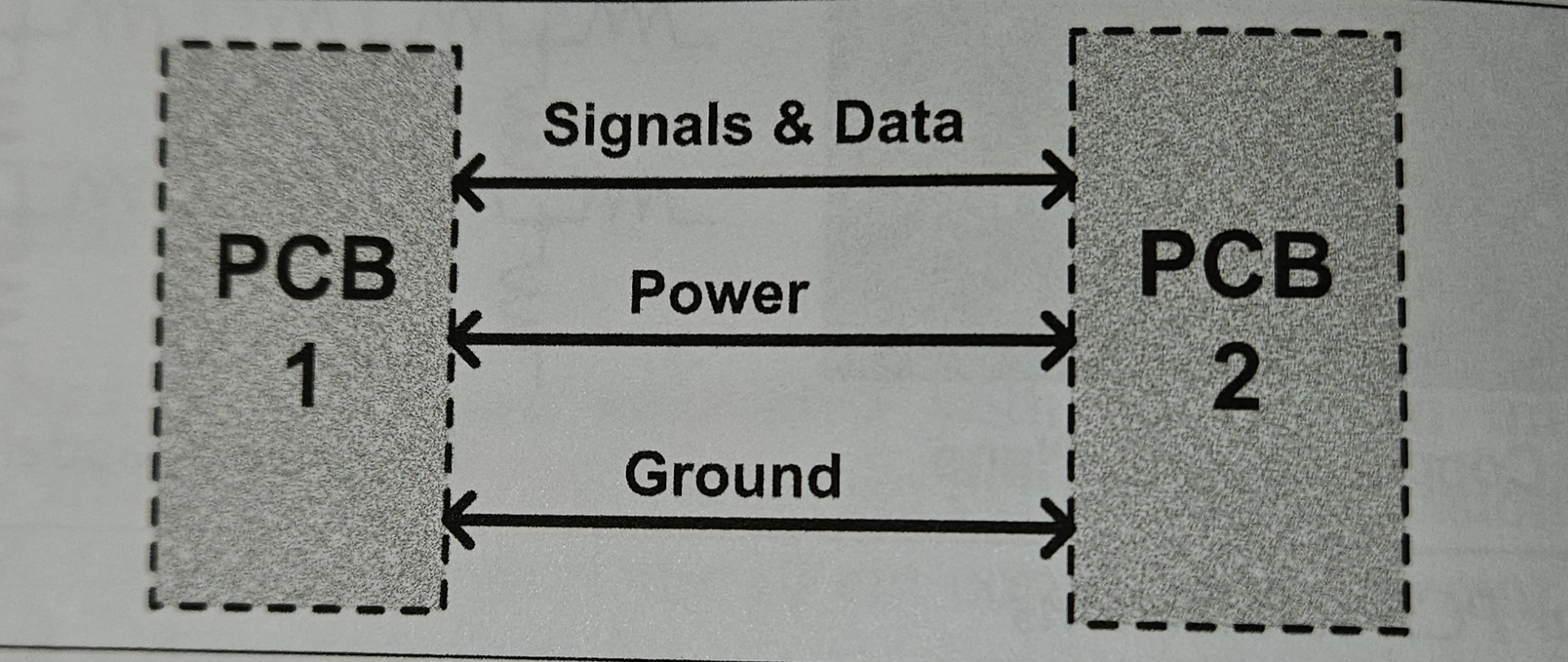
Connections between boards will exhibit signal integrity problems across all connections. Surges on power/ground wires will cause voltage variance between the separated boards. This will cause noise on any ground-referenced signal relative to local ground. External effects like EMI or electrostatic discharge (ESD) can also corrupt signal. Special effort is necessary to 'clean up' noisy raw power entering a board. Data and signals must pass between boards in a way that is not dependent on local ground or power supply.
Sending a communication signal to multiple locations can cause phase errors between reception points. In this connection there can be ditributed connection impedance, lead length, and capacitive receiver load. These will produce 5 different received phases in the given example. This is a common problem in clock-tree distribution, especially given high clock frequencies, many destinations, and long distances.
Tangent 3: Clock-tree distribution is the method by which a clock signal is distributed from a source to sequential components in a system like an integrated circuit (IC). There are several architectures for building and implementing clock-trees, but these will be covered later.
Designers often neglect interconnection issues until problems arise, but by then an expensive redesign will be necessary. With high current, long connections, or high frequencies, interconnection issues must be considered throughout the design process.
Emphasis in this series is on more modern systems that will be mass produced. Axial-lead components and through-hole devices are minimized in this setting. Most components then will be the surface-mount type.
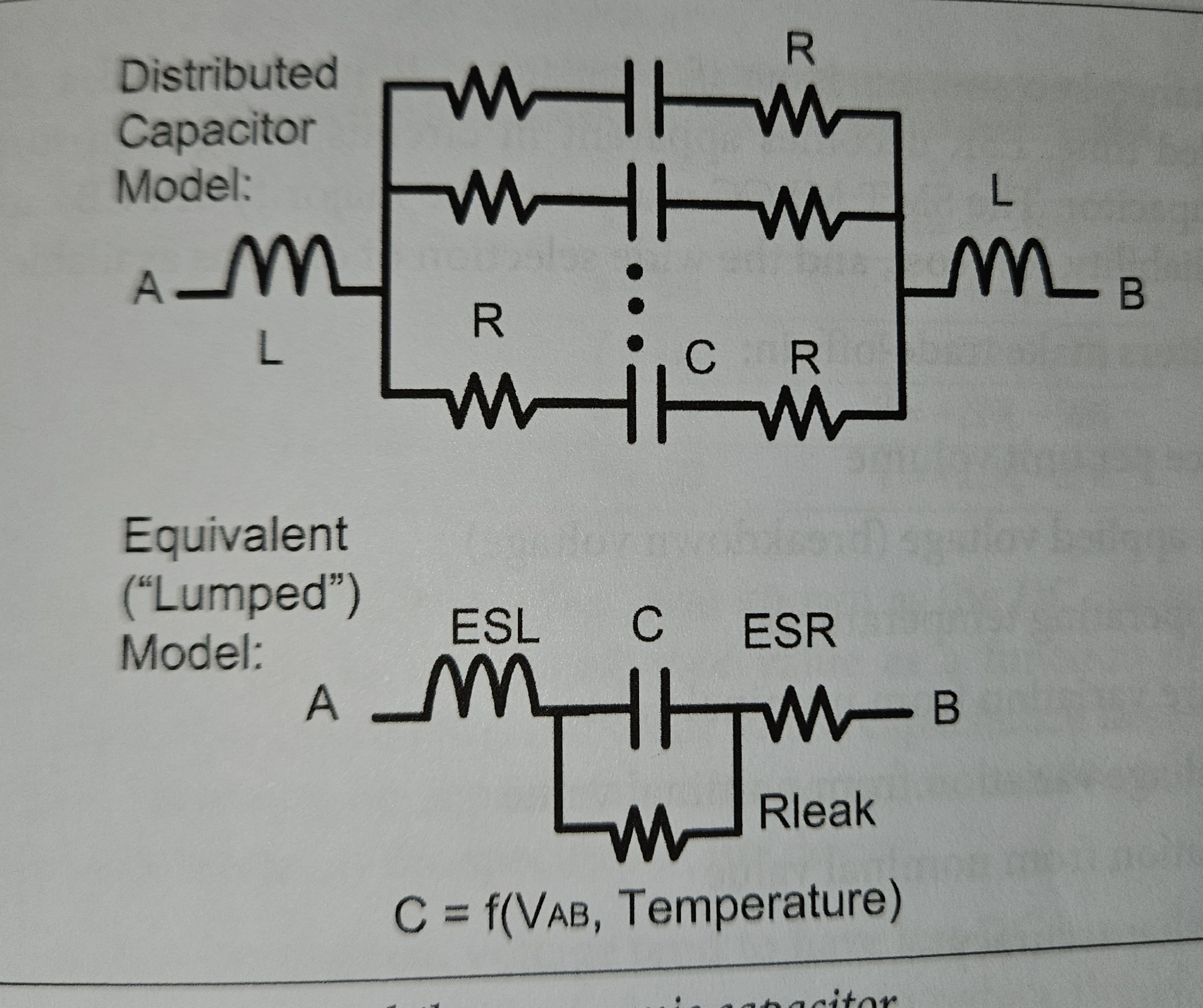
A surface-mount multi-layer capacitor has multple interleaved conducting and insulating layers. Actual capacitance is between adjacent plates. All plates carry some resistance, and interconnections have inductance. The distrubuted element model can be awkward to work with, so an equivalent model is generally sufficient and accurate.
The equivalent or lumped element model includes elements that model observed behavior. The device in the diagram has an Equivalent Series Inductance (ESL), Equivalent Series Resistance (ESR), a capacitor, and a leakage resistance. The main capacitor element can vary, mostly as a function fo temperature and applied voltage. Variability is due to the dielectric material between plates.
Depending on the application, some elements can be ignored, but in others they can limit device performance. Equivalent Series Inductance is important in radio-frequency circuits and high frequency power filters, but does not affect low-frequency performance. ESL with capacitance creates a self-resonant tuned circuit which limits the high-frequency response of the capacitor.
Leakage resistance is an issue when a capacitor is used to store a charge for an extended time. ESR manifests in circuits using high surge currents through a capacitor. The Surface Mount Technology Multi-Layer Ceramic Capacitor is used in the majority of modern PCB capacitors due to high reliability, low cost, and broad selection.
The tradeoffs of modern capacitors include:
These qualities are not mutually exclusive and there are multivariate interrelations between them.
SMT-MLCCs use several materials as dielectric. C0G, NP0 - capcitors designed for minimal temperature variance, minimal change from voltage bias. These sacrifice capacitance/volume in favor of high accuracy and stability. They are useful in tuned circuits and other applications that demand stability and accuracy.
X5R, X7R, Y5V, etc. - class 2 (see table) sacrifice voltage bias accuracy, thermal stability, in favor of greater capacitance per volume. Characteristics indicate minimum temp, maximum temp, value variance over temperature respectively.
These also have a DC voltage bias effect, or DC voltage charactaristic, which is a change in capacitance as a function of static applied DC voltage. Generally, capacitance decreases as bias voltage increases. Value can change up to 60% from rating. Capacitors with higher breakdown voltage have less DC bias effect for the same voltage change. This is useful if we dant to reduce voltage bias.
Aluminum Electrolytic Capacitors (AEC) are used in DC power supply fiters, and in other needs as large capacitance, small volume, and low cost packages. Poor high-frequency response, due to high ESI, so AECs are not suitable for RF use. AEC high frequency response can be supplemented with MLCCs. Limited function lifetime, fussy about temperature, significant ESR.
Tantalum and Aluminum Polymer Capacitors: High reliability, high function lifetime, can also have short service life.
Important considerations when selecting capacitors:
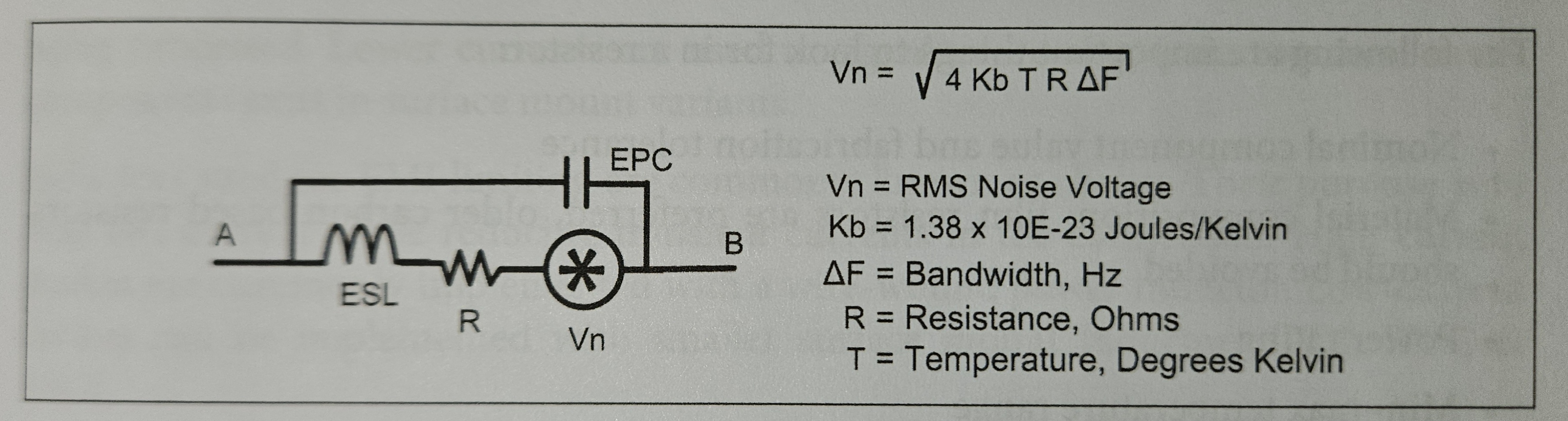
In addition to an 'ideal' resistance value, other elements must be considered.
In an ideal device, resistors should have a constant impedance over a frequency range. Due to EPC and ESL, impedance may change at higher frequencies. In DC applications EPC and ESL can be ignored. Multi-watt resistors are typically made of wound dire, and have significant ESL and EPC components. Most surface-mount resistors are film resistors, thick, thin, metal film, etc. Metal film generally produces less noise than carbon and thick film, but refer to datasheets to verify.
Thermal Noise or Johnson-Nyquist Noise: Thermal excitation of electrons in a resistive material. In most 'large-signal' applications, this is a non-issue. It becomes an issue in RF front-ends, communication channels, and low-amplitude radio, where signals may be measured in nanovolts.
Quick definitions: 'Large Signal' applications or circuits are designed to process large swings in voltage or current, and are more concerned with providing maximum power for an output load, rather than just voltage gain. An RF front-end is the circuitry in a radio antenna leading from the receiving antenna up to and including the mixing stage.
Some manufacturers produce gigaOhm resistors but these require special considerations. Dust and humidity can create lower impedance paths around the resistor. Generally, any resistor rated over 100kΩ demands environmental attention to prevent current taking alternate routes. Such resistors are not typically needed because circuits that demanded them have largely been replaced by more reliable digital equivalents.
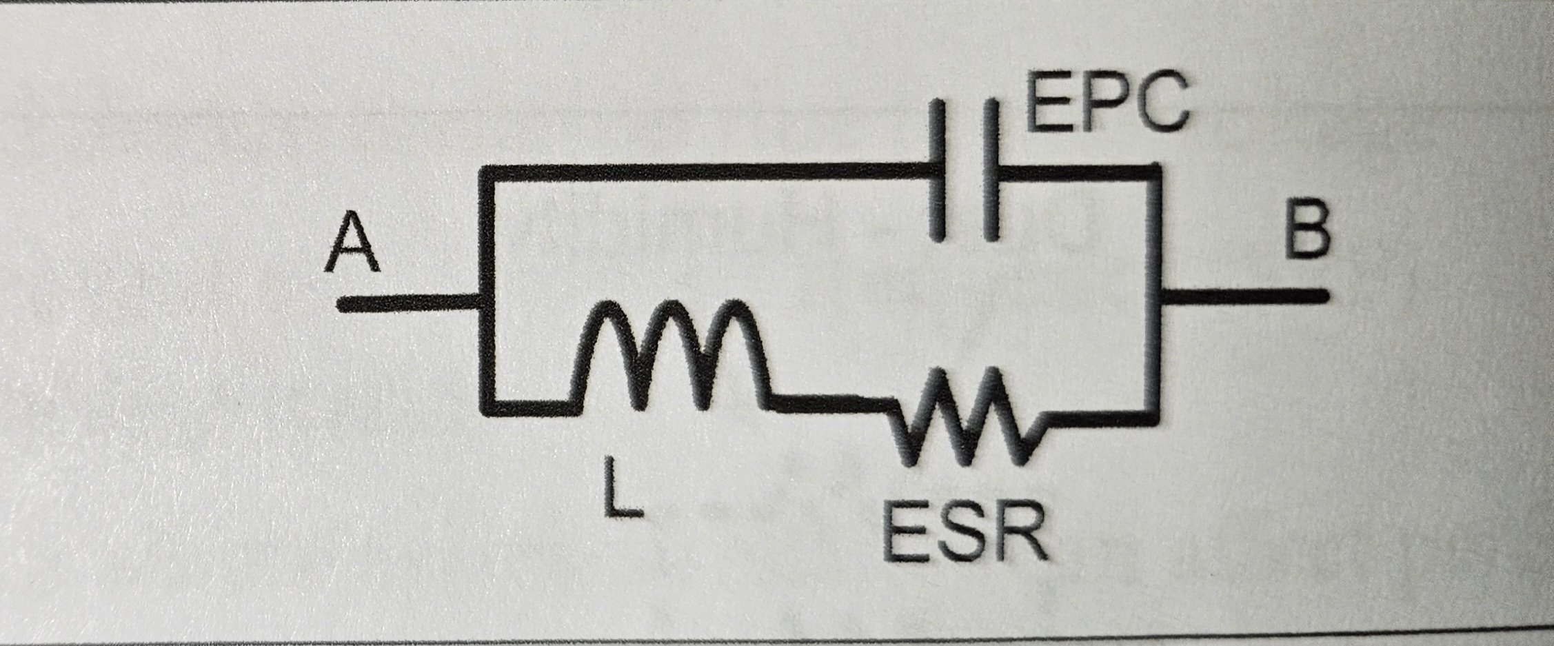
There is always some Equivalent Parallel Capacitance in inductors, which limits frequency ranges. With EPC and Inductance (L) in parallel, this resonates as a tank circuit, and looks like an open circuit at the self-resonance frequency. Below the self-resonance frequency (SRF), this device functions as a regular inductor. Above SRF, this device acts like a capacitor. Equivalent Series Resistance in this device defines a Quality Factor (Q) of the inductor when used as part of a filter. When used in a switching power converter, ESR limits power efficiency.
Inductors are regularly used for power conversion, RF signal processing, and limiting EMI. They are also used in switched-mode power conversion in both AC/DC and DC/DC power converters. The priorities on inductors in power conversion are: Maximum current, Saturation current, thermal range, and resistive loss. Switching converters have high current transients, so suitable devices are wire-wound on a magnetic core, with high current capability and low resistance loss.
In RF signal processing, inductors are used in tuned circuits and need consistent accuracy to produce a reliable frequency response. Priority here is a high quality-factor and component tolerance/accuracy, to ensure self-resonance does not interfere with signal processing. This is a low-current application, and many related inductors are surface-mount devices.
When limiting EMI, inductors are often called 'chokes'. These pass DC current and reduce transient currents in the conection. High-current chokes are typically made of wire-wound components. Low-current chokes can be implemented as a surface-mount device.
There is no ideal voltage source. An infinite source of current at a fixed voltage is purely theoretical. All sources have limitations.
Any detailed voltage source model must include Source Resistance, a Noise Component, and the voltage source as a dependent function of the output current or load. The goal of a design is to minimize source-resistance, noise, and dependence on current load.
Batteries have a limited capacity, and change in voltage output over time must be included in the model. Batteries also have current limitations, performance changes with age, and other limitations depending on type.
Noise characteristics are highly dependent on methods of voltage generation. Linear supplies and regulators are made for low-noise applications. Batteries tend to have low noise, but electrochemical processes can still produce noise, and a battery charger can introduce noise to an environment.
Switching power-supplies can be very efficient but produce commutation noise associated with voltager regulation. Commutation is the acoustic or electrical noise caused by the switching of current, often inside electric motors.
Digital systems don't often demand ultra-low-noise power, but any chip placed in a design must be investigated for 'noise on the power' limitations. 'Noise on the power' in this context refers to unwanted fluctuations in power that may reach and damage a given IC chip or similar sensitive component.
There is also no ideal current source.
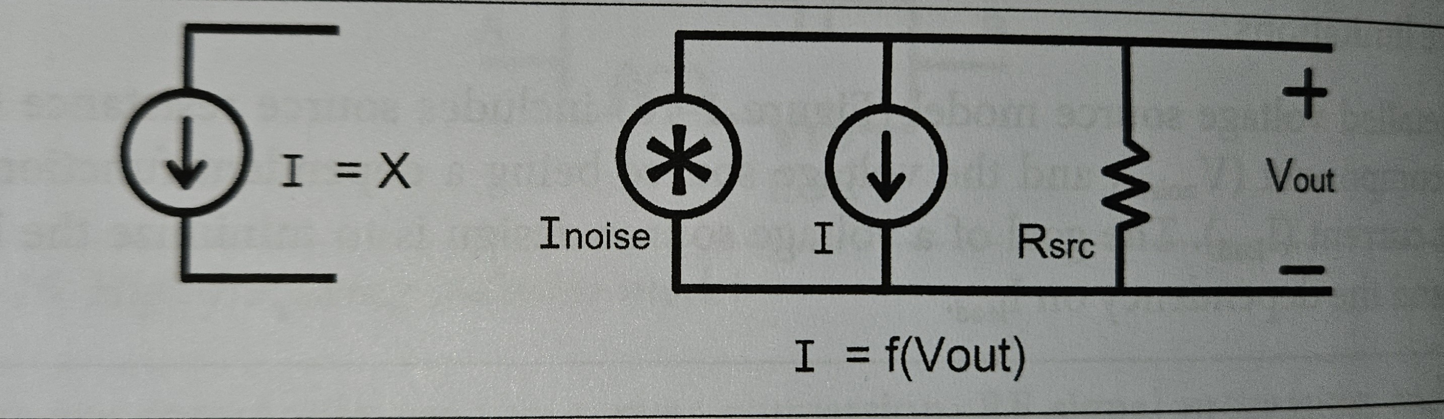
^Ideal versus Real current sources
Practical current sources have source resistance, noise, and output current as a dependent funtion of output voltage. Most sources have limited voltage range to ensure consistent current behavior. Discrete current sources are not used in system-on-a-chip design, but they are important in integrated circuits that are analog and mixed-signal types.
A Discrete Current Source uses some circuitry so deliver a constant current and meet requirements on current precision. These sources are often designed to work in a specific voltage range, outside of which function is not defined or guaranteed.
See Cascode
Mechanical switches can be problematic, especially if they are control inputs on a logic part. Contact bounce can create many on-off states in quick succession. Using a switch on a logic part requires that software account for bounce by waiting for stability before executing a state change.
Switches also have inductance, which adds impedance in a closed switch. 'Parasitic Capacitace' can allow signals to pass over an open switch. Contacts also have variable resistance, which can change with each switch cycle. This worsens with age as contacts get dirty or damaged by their environment.
Practical OP-Amps have limitations that affect performance. They need power, ground, and they can be noise-sensitive on those connections. Their output has impedance, and output voltage is limited by supply voltage. Gain is never infinite, but open-loop gain is typically 80dB. Open-loop gain is the gain of an amplifier when it receives no feedback.
Gain response over a range of frequencies will be limited by bandwidth and additive phase response. Since an Op-Amp is intended to work in a closed feedback system, high frequency gain has to be limited to keep it stable in a feedback configuration. Because of frequency compensation, op-amps may be less than ideal for high frequency applications.
Input capacitance creates a loading effect, which can affect high-frequency performance. Op-amps with bi-polar transistors will have input bias current. A bi-polar transistor is a 3-terminal transistor that uses a small current on one terminal to control a much larger current over the other two. Input transistors are not perfectly matched and may produce equivalent input offset voltage, usually 1-10mV. This can be problematic for small signals or high-gain closed-loop setups. Internal circuitry also creates noise, modeled as an Input Referred Noise source. Many of these are not problems when working with 'large' signals, but going for high gain and high bandwidth, or using sub-mV signals will show limitations.
A voltage comparator is a circuit that takes two input voltages and produces a binary output voltage as a result. They are sensitive to noise on their power and ground connections, and they can have input loading capacitance, input referred noise, and input offset voltage similar to op-amps. These are typically applied against a fixed reference voltage, and one-sided models usually suffice.
The difference between an op-amp and a voltage comparator is that an op-amp is in an analog feedback loop, and a comparator is not. Gain in a comparator is higher, around 100dB, with no internal frequency compensation, and the output is digital. There is variable time-response included, as input/output time can depend on the amplitude of the input signal. Small signals with minimal crossover voltage are slower to propagate than large voltage transitions.
Digital devices are generally more resilient to noise than analog devices. For example, communications between Field Programmable Gate Arrays (FPGAs) and microcontrollers share common power and ground. Connections here have distributed inductance, due to the parasitic inductance effect. Depending on other connections, current drawn or added can cause communication connections to fluctuate. The magnitude of a fluctuation can differ by its location in the network. The tolerable range for a fluctuation is determined by gate transistors, but stable power and ground must be a priority.
Complimentary Metal-Oxide-Semiconductors (CMOS) have a transistor threshold voltage around a third of the power-supply voltage, they can tolerate power/ground instability of up to 20% from their nominal level before creating false states. Commercial products specify acceptable voltages for high and low logic states, which also indicate the tolerable power/ground variance. A clean two-state signal at one location can be corrupted by unstable power/ground at output and other locations, completely losing the original signal.
False-state Generation: In a Clocked System, two devices talk at the same frequency, but have separate clocks. Though the clocks run at the same frequency, they are not linked, and can phase apart. Phasing can violate setup and hold times, and can cause data errors.
Asynchronous logic should be avoided for unpredictable outputs and glitches. Synchronous logic prevents errors caused by propagation delay. Digital functionality can suffer due to the analog characteristics of digital signals; High data rates, transmission resistance, capacitance load on transmission paths.
Signal Drivers and Receivers can have interconnect impedance, resistance at PCB, inductance, and capacitance. A CMOS logic output driver can be modeled as a pair of switches and a resistor. Output resistance can be from 10 to 80 Ohms. Receiver input can act as capacitance, due to large, high-current ESD protective circuits. 2 to 10pF is common for logic gates. Except for interconnect inductance, there is potential for an RC low-pass filter at every digital interconnection.
In more detailed models, frequency limitations are more apparent. Driver resistance and capacitance distort what would be a more ideal square wave function. At low frequencies there is time for the transient to pass, but at higher frequencies the transient cannot pass before the state changes direction. The RC time constant is the same, but well-defined logic states are not reached.
A system will fail when voltage limits are violated or when setup and hold times on flip-flops are not met. Ground-referenced logic often fails when used for high frequency communications, and differential signals are used at high data rates to minimize that limitation.
Any circuit can cause undesired side-effects in normal operation. Many systems cause noise with signals that radiate externally. Internal parts can interfere with one another. Poorly designed systems can be sensitive to external EMI. Signal Integrity, RF Interference, Electromagnetic Compatibility (EMC), electronic noise, RF immunity, EM shielding, Radiated Emissions, and crosstalk must be considered.
Consider a 10cm connection again. This can create radiated emissions as an ideal, 1/4 wavelength antenna at about 700MHz. A 100MHz clock would transmit on its 7th harmonic for this antenna, making this connection a radio transmitter. All frequencies would radiate from the connection, but at a range of efficiencies.
Radiated emissions are problematic when produced by computers or any large amount of high-frequency digital circuitry. The FCC and other regulators restrict what EMI can be produced by devices, intended to minimize interaction problems.
There can also be EMI between internal circuits (crosstalk). Noise can be capacitive or magnetic, and can take both paths. This is a common problem with digital signals, especially at high frequencies, and can be coupled to an unconnected circuit path.
Be aware of the limitations and non-ideal nature of electronics. Many engineers learn this from costly failures. Learning from experience is valuable, but it is not the most efficient way to learn these lessons. Later, these limitations will be addressed with real-world solutions.